
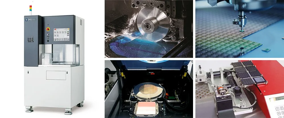
Our world-class DISCO automatic dicing systems process 300mm wafers across diverse materials—silicon, MEMS, GaN, GaAs, glass, and more. The complete processing suite includes backgrind, polish, first and second optical AOI, and automated pick-and-place into your preferred packaging.
Wafer probe services available upon request. Blade specifications are tailored to each substrate’s material and thickness for optimal results. Diced wafers can be shipped on wafer frame, or sorted into waffle pack or Gel-Pak. For more information you can call or send us an email to discuss your wafer dicing needs.
WAFER INSPECTION
Visual die inspection identifies and removes all mechanical defects from post-fabrication processes before shipment, meeting MIL-STD-883 (Class B or Class S) standards. Using AOI (automated optical inspection) or high-magnification microscopes, we detect chip-outs, cracks, passivation voids, surface scratches, metal bridging, embedded foreign material, and contamination to ensure only defect-free die are delivered.
MIL-STD-883 (Class B or Class S)
AOI (automated optical inspection) and manual visual using high magnification microscopes
Customer-specific requirements
DIE SORTING
Full die sorting and pick-and-place capabilities with Automated Optical Inspection (AOI), wafer test capabilities, speed/temperature binning, “in family” data segregation, and Known Good Die verification for optimal yield.
Diced wafers can be shipped on wafer frame, or sorted into waffle pack or Gel-Pak.